How to Design RF Trace Tapers (With Free Calculator!)

11:58
PCB Layer Reduction on an nRF52 Module: Concepts & Walkthrough

22:26
Samsung Galaxy Fit 3 in India, HMD Barbie Flip phone, Xiaomi 14, 14 Ultra, Watch 2 global | TVT 1291

20:29
PCB Trace Inductance Deep Dive - When to Widen Traces

1:35:32
PCB Antenna - How To Design, Measure And Tune

48:34
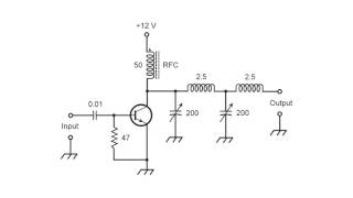
RF Design-7: Broadband and Multi-Stage Impedance Matching Design

4:05
Altium How to Create Ground Plane GND - from the lab

13:43
Guard Traces & Crosstalk | A Follow-up

8:41