Meaning of STH CPH TP POL SOE STB and relationship between TCON Gamma and source driver
23:49
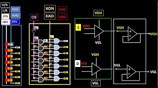
What does it mean on a TCON board CPV CKV CKVB STV STVP OE XAO RL UD VGH VGL
13:54
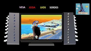
Video signal transmission between motherboard and Tcon via LVDS. VESA and JEIDA standard

26:40
Signification de STH CPH TP POL SOE STB et relation entre le Gamma du TCON avec le source driver

16:17
Rearchitecting the 6502

44:21
Op-Amps - Using Operational Amplifiers
14:43
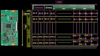
Organization of the pixels in LCD screen and the different circuits of their control from the TCON

18:43
The Gamma chip of the TCON board and the role of the opamp configured as a voltage follower

54:49