IV characteristics of schottky diode at zero bias

28:59
Metal semiconductor contact, tunneling barrier and specific contact resistance

9:22
DAY 27 OF 50DAYS PHYSICS CHALLENGE - ALL PHASOR DIAGRAM -8168403177- LCR CIRCUIT AND IMPEDANCE

24:53
Metal semiconductor junction, Schottky diode

13:47
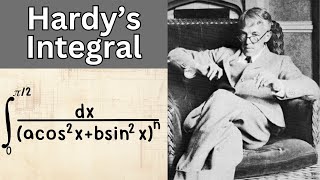
Hardy's Integral

44:42
Darlington Emitter Follower circuit with derivations

24:39
Formation of Energy Bands

29:26
emitter, collector and base currents in BJT

13:05