ASIC Interview Questions | CMOS Inverter Transfer Characteristics (VTC) | Regions | Noise-margins

20:16
Inverter - 2 - Voltage Transfer Characteristics

28:09
CpE100 Module3b - Noise Margins - Dr. Harris

12:26
ASIC Interview Questions | Power Dissipation in CMOS Circuits | Dynamic| Short-circuit | Leakage

17:05
Inverter - 6 - Noise Margin Analysis-1

8:23
Digital Design Interview Questions | Setup and Hold Time in Flip-Flop and Latch | Static Timing
15:40
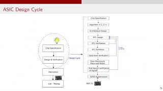
ASIC | Digital Interview Questions | ASIC design flow | RTL to GDSII | Synthesis | Verification

16:06
Noise Margin and Fan-out of Logic Gate Explained

6:53