Antenna Effect Prevention Techniques in VLSI Design

15:43
Electromigration in VLSI Design | What is electromigration | How to prevent Electromigration

21:25
IR Drop issue in VLSI | What is IR drop in ASIC | Why IR Drop | Effects of IR Drop

12:58
Well Tap Cell | Tap Cell | Use of Tap Cells | Placement of Tap Cell | Layout of Tap Cell

13:00
Antenna Effects | Physical Verification | Back To Basics

18:19
Antenna effect in VLSI Fabrication | Plasma Induced Gate Oxide Damage | Plasma Etching

15:21
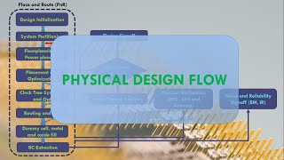
Physical Design Flow | VLSI back end | IC Design

29:50
On-Chip Variation in VLSI | OCV | Why OCV occur | How to take care of OCV | AOCV | POCV

9:50