Altium Designer Tutorial 37: IPC specification for plated through hole (Via)

1:24:28
Altium Designer Tutorial 39: PCB Layout 10 design rules.
25:39
Altium Designer Tutorial 41: How to create a Schematic Template in Altium Designer 24.10.

19:00
How to Use Blind and Buried Vias

27:58
Altium Designer Tutorial 42: How to create TSSOP-14 Symbol and footprint in Altium Integrated Lib.

16:28
Altium Designer Tutorial 40 : Place 3D Step model using Snap point or position 3D Body function.

16:10
When to Use Via in Pad
25:54
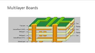
Introduction to Basic Concepts in PCB Design

7:50