VGH and VGL production mode by the TCON board. The charge pump converter.

9:45
Internal structure of a liquid crystal or LCD TV screen
23:49
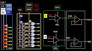
What does it mean on a TCON board CPV CKV CKVB STV STVP OE XAO RL UD VGH VGL

5:03
VDD and AVVD voltage production mode by the TCON board . The Buck and boost converters.

25:33
Que signifie sur une carte TCON les termes CPV CKV CKVB STV STVP OE XAO RL UD VGH VGL

5:11
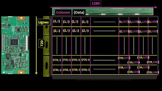
Geometry of pixels in an LCD screen and their control by the Gate driver
10:54
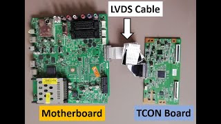
Meaning of the LVDS used between the motherboard of an LCD TV and the TCON board
14:43
Organization of the pixels in LCD screen and the different circuits of their control from the TCON

18:43